标签:15 hierarchy 31 module verilog output input sum
Problem 19:Module
注意到程序开头都是 module,意味着我们写的程序都是一个模块电路
模块与模块之间构成了层级。
模块例化的基本语法:

module mod_a ( input in1, input in2, output out );//
    // Module body
endmodule
顶层模块的下层模块 mod_a 相当于一个黑盒子,里面什么东西并不重要,重要的是输入输出端口。
模块信号连接的两种方式
-
按端口顺序
mod_a instance1(wa,wb,wc);//模块名 实例名(定义连接 port 的信号
//wa,wb,wc分别连接到模块的第一个端口(in1),第二个端口(in2),第三个端口(out)。
这里的端口顺序指的是模块端口的定义顺序,一旦端口列表顺序发生改变,所有模块中的实例化中的端口都需要改变
-
按端口名称连接端口
mod_a instance1(.out(wc),.in1(wa),.in2(wb));//根据端口名称指定外部信号的连接,和端口定义的顺序完全没有关系
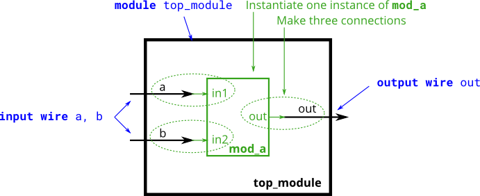
module top_module ( input a, input b, output out );
        mod_a U_mod_a(
          .in1(a)
        , .in2(b)
        , .out(out));
    //mod_a U_mod_a(a, .b, out); //使用按照端口顺序的方式 声明信号连接
endmodule
Problem 20: Connecting ports by position(Module pos)
给出一个 4 输入,2 输出的 mod_a 模块、
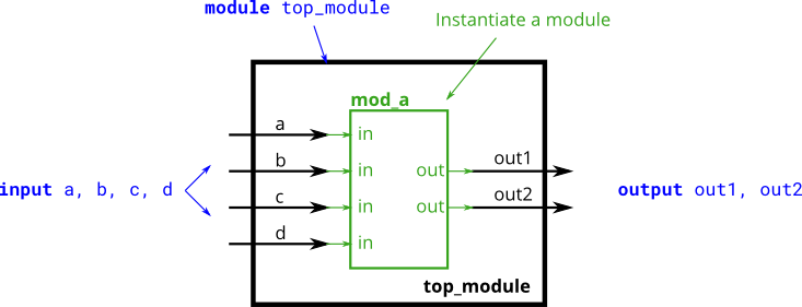
给出的模块如下:
module mod_a ( output, output, input, input, input, input );//只标注输入输出端口而没有名字是不规范的,应该要赋予每个端口一个名字
module top_module (
    input a,
    input b,
    input c,
    input d,
    output out1,
    output out2
);

    mod_a name(out1,out2,a,b,c,d);//这里题目并没有给出输入输出端口的名字,所以只能按照顺序来连接

endmodule
Problem 21:Connecting ports by name(Module name)
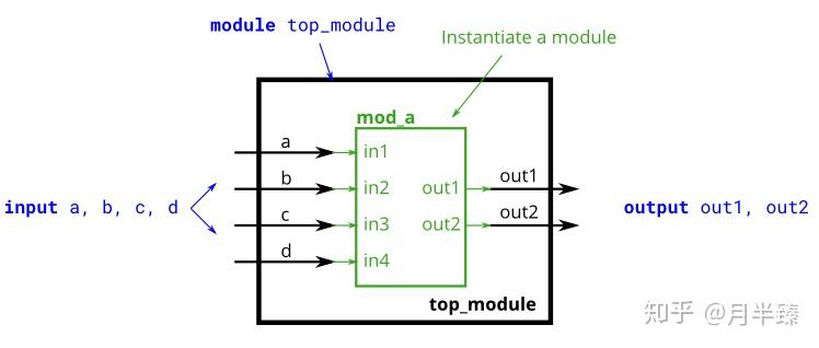
给出的模块如下:
module mod_a ( output out1, output out2, input in1, input in2, input in3, input in4);//这里给出了每个端口的名称
module top_module (
    input a,
    input b,
    input c,
    input d,
    output out1,
    output out2
);

    mod_a name(
        .out1(out1),
        .out2(out2),
        .in1(a),
        .in2(b),
        .in3(c),
        .in4(d));//这里按照模块端口名称进行连接,可以不用按顺序
endmodule
但如果按题目给出的顺序写成如下,会报错:
mod_a name(out1,out2,a,b,c,d);
(猜测是因为题目给的模块顺序发生的改变,不知道内部什么结构,所以有点难调)
Problem 22:Three modules(Module shift)
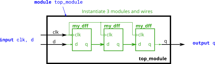
给出一个名为 my_dff 的模块,包含两个输入和一个输出
module my_dff ( input clk, input d, output q );
module top_module ( input clk, input d, output q );
    wire m,n;
    my_dff name1(.clk(clk),.d(d),.q(m));//对my_dff进行了三次实例化,用了三个不同的名字(name1,name2,name3)

    my_dff name2(.clk(clk),.d(m),.q(n));//端口用了名称定义的方式,建议少用顺序定义的方式
    my_dff name3(.clk(clk),.d(n),.q(q));
endmodule
Problem 23:Module and vectors(Module shift8)
向量可以代替单根连接线作为模块的端口,在连接的时候也是向量连接,而不是单根导线
当端口的向量长度和连接的导线不匹配时,会导致向量的零填充或截断,
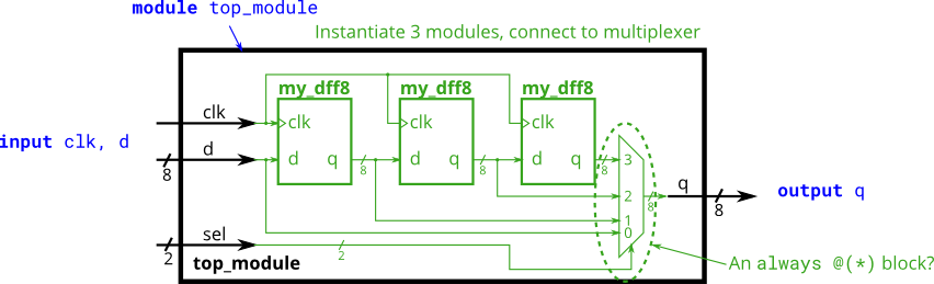
给出一个模块,包含两个输入和一个输出,实现一个 8bit 的 D 触发器。实例化三个模块,并连接在一起,形成一个长度为 3 的 8bit 的移位寄存器。
再加入一个 4 选 1 多路复用器,根据输入的 sel[1:0]选择要输出的内容:输入 D 的值,第一个 D 触发器之后的值……相当于是选择输入延迟的周期数,0~3 个时钟周期不等
给出:
module my_dff8 ( input clk, input [7:0] d, output [7:0] q );
实现:
module top_module (
	input clk,
	input [7:0] d,
	input [1:0] sel,
	output reg [7:0] q
);

	wire [7:0] o1, o2, o3;		// 声明每一个触发器的输出

	// Instantiate three my_dff8s
	my_dff8 d1 ( clk, d, o1 );
	my_dff8 d2 ( clk, o1, o2 );
	my_dff8 d3 ( clk, o2, o3 );

	// 这是实现4选1选择器的一种方法
	always @(*)		// 组合逻辑always块
		case(sel)
			2'h0: q = d;
			2'h1: q = o1;
			2'h2: q = o2;
			2'h3: q = o3;
		endcase

endmodule
Problem 24:Adder 1 (Module add)
给出一个 16bit 加法器模块 add16,实例化两个 add16 以达到 32bit 加法器。
原理:一个 add16 模块计算结果的低 16 位,另一个 add16 模块接受第一个的进位后计算结果的高 16 位。
给出:
module add16 ( input[15:0] a, input[15:0] b, input cin, output[15:0] sum, output cout );
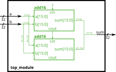
module top_module(
    input [31:0] a,
    input [31:0] b,
    output [31:0] sum
);
    wire cout;
    add16 c1(.a(a[15:0])
             ,.b(b[15:0])
             ,.cin(0)
             ,.sum(sum[15:0])
             ,.cout(cout)
            );
    add16 c2(.a(a[31:16])
             ,.b(b[31:16])
             ,.cin(cout)
             ,.sum(sum[31:16])
             ,.cout()
            );
endmodule
Problem 25:Adder 2(Module fadd)
描述一个具有两级层次结构的电路,实例化两个 add16 模块,每个 add16 中实例化 16 个 add1 实例。
给出:
module add16 ( input[15:0] a, input[15:0] b, input cin, output[15:0] sum, output cout );
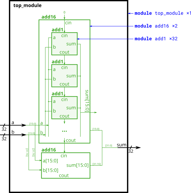
在每个 add16 中,实例化了 16 个全加器去执行加法操作,需要自己编写并声明。
全加器的逻辑表达式
实现
module top_module (
    input [31:0] a,
    input [31:0] b,
    output [31:0] sum
);//
wire carry;
    add16 a1(.a(a[15:0])
             ,.b(b[15:0])
             ,.cin(0)
             ,.sum(sum[15:0])
             ,.cout(carry)
            );
    add16 a2(.a(a[31:16])
             ,.b(b[31:16])
             ,.cin(carry)
             ,.sum(sum[31:16])
             ,.cout()
    );
endmodule

module add1 ( input a, input b, input cin,output sum, output cout );

// Full adder module here
	assign sum=a^b^cin;
    assign cout=(a&b)|(a&cin)|(b&cin);

endmodule
Problem 26:Carry-select adder(Module cseladd)
上面一个实现的加法器叫做行波进位加法器(RCA:Ripple-Carry Adder)
这种加法器的缺点:计算进位输出延迟比较大。
改进该加法器:第一级加法器保持不变,第二个加法器实现两个,一个假设进位为 0,另一个假设进位为 1,然后用第一级结果和 2 选 1 选择器来选择哪一种结果是正确的。
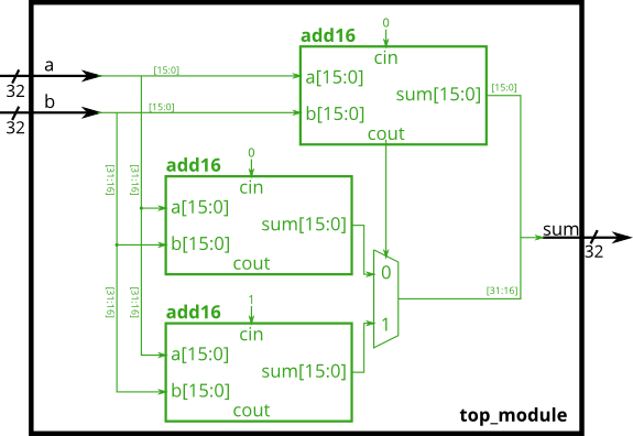
给出 add16 模块:
module add16 ( input[15:0] a, input[15:0] b, input cin, output[15:0] sum, output cout );
实现:
module top_module(
    input [31:0] a,
    input [31:0] b,
    output [31:0] sum
);
    wire carry;
    wire [31:16] sum0,sum1;
    add16 c1(.a(a[15:0])
             ,.b(b[15:0])
             ,.cin(0)
             ,.sum(sum[15:0])
             ,.cout(carry)
            );
    add16 c2(.a(a[31:16])
             ,.b(b[31:16])
             ,.cin(0)
             ,.sum(sum0[31:16])
             ,.cout());

    add16 c3(.a(a[31:16])
             ,.b(b[31:16])
             ,.cin(1)
             ,.sum(sum1[31:16])
             ,.cout());

    assign sum[31:16]=carry?sum1:sum0;
endmodule
以上是进位加法器(CSA:Carry-Select Adder),对比上一题的行波进位,加法器延迟小一半,但增多了 50% 的逻辑资源。
Problem 27:Adder–subtractor (Module addsub)
加减法器可以通过加法器去实现,对其中一个数取相反数(对输入数据取反,然后加 1)。
最终结果是一个可以执行以下两个操作的电路:a+b+0 和 a+~ b+1
给出 16bit 加法器模块:
module add16 ( input[15:0] a, input[15:0] b, input cin, output[15:0] sum, output cout );
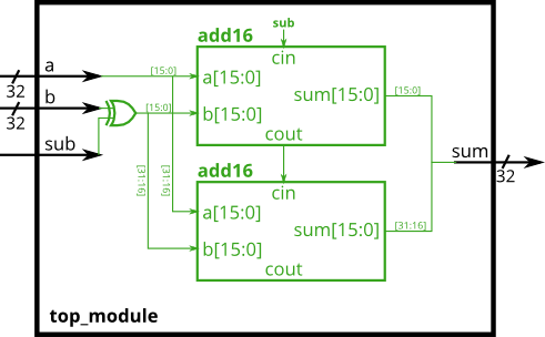
module top_module(
    input [31:0] a,
    input [31:0] b,
    input sub,
    output [31:0] sum
);
    wire carry;
    wire [31:0]b1;
    assign b1=b^{32{sub}};//当sub=1时,使用32位的异或门对B进行取反
    add16 c1(.a(a[15:0])
              ,.b(b1[15:0])
           ,.cin(sub)
           ,.sum(sum[15:0])
           ,.cout(carry)
          );
    add16 c2(.a(a[31:16])
             ,.b(b1[31:16])
             ,.cin(carry)
             ,.sum(sum[31:16])
             ,.cout()
            );
endmodule
- 减去一个数等于加上这个数的补码(代码中的按位取反再加 1)
标签:15,hierarchy,31,module,verilog,output,input,sum 来源: https://www.cnblogs.com/zjj666/p/15614833.html
本站声明: 1. iCode9 技术分享网(下文简称本站)提供的所有内容,仅供技术学习、探讨和分享; 2. 关于本站的所有留言、评论、转载及引用,纯属内容发起人的个人观点,与本站观点和立场无关; 3. 关于本站的所有言论和文字,纯属内容发起人的个人观点,与本站观点和立场无关; 4. 本站文章均是网友提供,不完全保证技术分享内容的完整性、准确性、时效性、风险性和版权归属;如您发现该文章侵犯了您的权益,可联系我们第一时间进行删除; 5. 本站为非盈利性的个人网站,所有内容不会用来进行牟利,也不会利用任何形式的广告来间接获益,纯粹是为了广大技术爱好者提供技术内容和技术思想的分享性交流网站。